
製品情報
AFM/SPM校正用グレーティング
製品詳細

分野
- 分析・検査
- 計測
- イメージング
- バイオ・ライフサイエンス
- 教育
メーカー
TipsNano
(エストニア)
正規代理店
概要
原子間力顕微鏡(AFM)、走査型プローブ顕微鏡(SPM)の各種校正や評価にお使いいただける校正用グレーティングです。校正の種類や評価に応じて、適切なグレーティングをご選択頂けます。
より安価でご案内できる、複数のグレーティングをまとめたセットもございます。
特長
・豊富なラインアップ 9種
・XYZ軸校正やティップ形状評価など
・低価格
・複数のグレーティングをまとめた安価なセットあり
仕様
■校正用グレーティングモデル
Model TGZ1
Application ・Z軸校正用
Structure step - SiO2, bottom – Si

Pattern type 2-Dimensional
Period 3 ± 0.05 µm
Height 20,0 ± 1.5 nm*
Chip size 5 x 5 x 0.5 mm
Effective area central square 3 x 3 mm
| Model | TGZ2 |
|---|---|
| Application | ・Z軸校正用 |
| Structure | step - SiO2, bottom - Si |
| Pattern type | 2-Dimensional |
| Period | 3 ± 0.05 µm |
| Height | 110 ± 2 nm* |
| Chip size | 5 x 5 x 0.5 mm |
| Effective area | central square 3 x 3 mm |
| Model | TGZ3 |
|---|---|
| Application | ・Z軸校正用 |
| Structure | step - SiO2, bottom - Si |
| Pattern type | 2-Dimensional |
| Period | 3 ± 0.05 µm |
| Height | 520 ± 3 nm* |
| Chip size | 5 x 5 x 0.5 mm |
| Effective area | central square 3 x 3 mm |
| Model | TGZ4 |
|---|---|
| Application | ・Z軸校正用 |
| Structure | step - SiO2, bottom - Si |
| Pattern type | 2-Dimensional |
| Period | 3 ± 0.05 µm |
| Height | 1517 ± 20 nm* |
| Chip size | 5 x 5 x 0.5 mm |
| Effective area | central square 3 x 3 mm |
| Model | TGQ1 |
|---|---|
| Application | ・XYZ軸の同時校正用 ・スキャナーの水平校正 ・水平ノンリニアリティ、ヒステリシス、クリープ、 クロスカップリングエフェクトの検出 |
| Structure | step - SiO2, bottom - Si |
| Pattern type | 3-Dimensional array of rectangulars |
| Period | 3 ± 0.05 µm |
| Height | 20 ± 1.5 nm* |
| Rectangles side size | 1.5 ± 0.35 µm |
| Chip size | 5 x 5 x 0.5 mm |
| Effective area | central square 3 x 3 mm |
(* 300個のバッチから取り出した5個のステップ高の平均値を仕様に用いているため、ステップ高の仕様数値がバッチごとに変更されます。仕様数値の±10%を公差としています。)
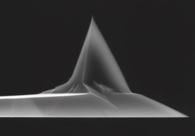
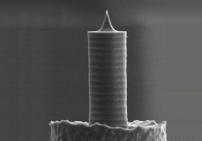
| Model | TGT1 |
|---|---|
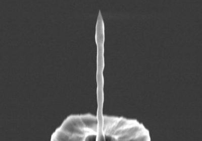
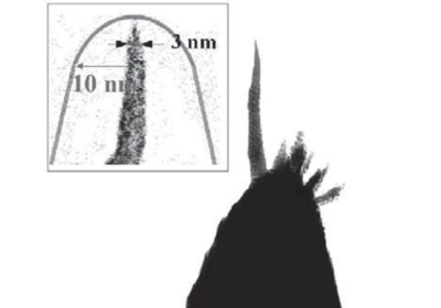
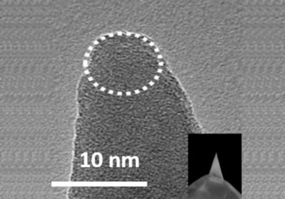
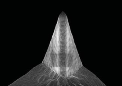
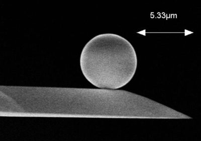
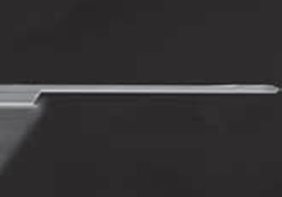
| Application | ・AFM/SPMプローブのティップの形状と鋭さの評価 ・ティップの劣化・汚染防止 |
| Structure | the grating is formed on Si wafer top surface |
| Pattern type | 3-D array of sharp tips |
| Period | 3 ± 0.05 µm |
| Height | 0.3 - 0.5 µm |
| Chip size | 5 x 5 x 0.5 mm |
| Effective area | central square 2 x 2 mm |
| Tip angle | 50 ± 10 degrees (on the very tip end) |
| Tip curvature radius | ≤ 10 nm |
| Diagonal period | 2.12 µm |
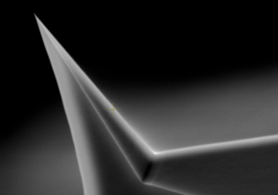
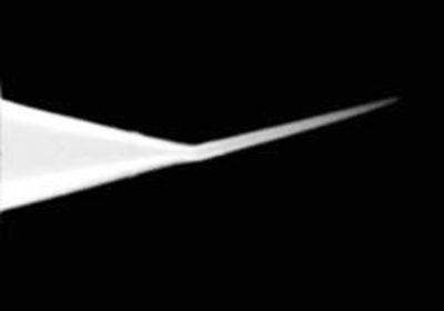
| Model | TGG1 |
|---|---|
| Application | ・X軸またはY軸の校正 ・水平または垂直スキャナーのノンリニアリティ検出 ・角変形の検出 ・ティップ特性評価 |
| Structure | Si |
| Pattern type | 1- D array of triangular steps (in X or Y direction) having precise linear and angular sizes |
| Period | 3 ± 0.05 µm |
| Chip size | 5 x 5 x 0.5 mm |
| Effective area | central square 3 x 3 mm |
| Edge angle | 70 degrees |
| Edge radius | ≤ 10 nm |
| Model | TGX1 |
|---|---|
| Application | ・水平スキャナーの校正 ・水平ノンリニアリティ、ヒステリシス、クリープ、 クロスカップリングエフェクトの検出 ・ティップの鋭さの決定 |
| Structure | Si |
| Pattern type | chessboard-like array of square pillars with sharp undercut edges |
| Period | 3 ± 0.05 µm |
| Height | ~ 0.6 µm |
| Chip size | 5 x 5 x 0.5 mm |
| Effective area | central square 3 x 3 mm |
| Edge curvature radius | less then 10 nm |
| Model | TDG01 |
|---|---|
| Application | ・X軸またはY軸の校正 (278nm period) |
| Structure | the grating is formed on the chalcogenide glass coated by Al |
| Pattern type | parallel ridges in X or Y direction, 1-Dimensional |
| Period | 278 ± 1 nm |
| Height | > 55 nm |
| Chip size | diameter 12.5 mm, thickness - 2,5 mm |
| Effective area | central diameter 9 mm |
■ グレーティングセット
| グレーティングセット | 内容 |
|---|---|
| TGS1 | TGZ1、TGZ2、TGZ3 |
| TGS2 | TGZ1、TGZ2、TGZ3、TGT1、TGG1、TGX1 |
| TGS1F | TGZ1、TGZ2、TGZ3、TGZ4 |
| TGSFull | TGZ1、TGZ2、TGZ3、TGQ1、TGT1、TGG1、TGX1 |
| TGSFull+ | TGZ1、TGZ2、TGZ3、TGQ1、TGT1、TGG1、TGX1、TDG01 |
| TGS1_PTB | TGZ1、TGZ2、TGZ3 (PTB校正証明書付き) |
各資料
製品に関するご質問・御見積など、お気軽にお問い合わせください
03-6659-7541
関連製品


- この製品を検討
リストに追加する - この製品について
お問い合わせする